
The Circuit: Designing for Low Power, Clean Logic, and Physical Constraints
In Part 1, I explained why I tore out the original “transistor-and-hope” lighting circuit from my Book Nook kit.
In Part 2, I went through the firmware architecture around watchdog sleep, pin-change interrupts, and ultra-low standby current.
Now it’s time for the hardware — the decisions behind it, why I chose active-low, why the LED is low-side switched, and how the entire board was physically shaped around a double-AAA battery compartment.
The Physical Constraints That Drove Everything
The board was designed to be DIY friendly, sit along the edge of a dual AAA battery case, and fit into the original compartment. That constraint dictated:
- Narrow, elongated PCB
- Through-hole components for easy DIY, including modifications
- All connectors aligned along one side
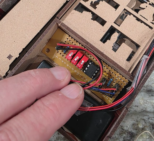
The mechanical constraints had to come first, and the design had to support the low-power goal of the project. I wanted to stick with through-hold components because that’s a lot more accessible to the average DIYer, and allows pretty simple updates for things like LED brightness (with a different R1 resistor) or even repurposing a switch. I also wanted it to work well on a perfboard, but because I like to overdo stuff like this, I wanted to design a custom PCB for it, too.
There’s no ISP header here because that would add a bit of complexity and result in a larger footprint. Maybe it would have worked with SMT components, but that would be a bit less accessible from a DIY perspective, so I’m just going to solder on an 8-pin DIP socket to make it easy to update the firmware out of circuit. If you’re doing this project or a project like this, you probably already have a way to program these MCUs out of circuit.
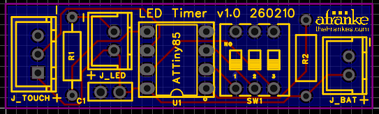
High-Level Architecture
The core of the design is the ATtiny85, which handles It handles touch input, DIP switch configuration, LED control, and auto-off timing. Around it, the circuit is intentionally sparse:
- R1 — LED current limiting
- R2 — pull-up resistor
- C1 — 100nF decoupling capacitor
- SW1 — DIP switch
- Headers for battery, LED, and touch sensor
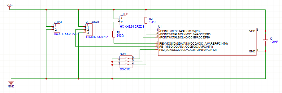
Why Active-Low Signals?
I wired the inputs active LOW for a couple of reasons.
1. Internal Pull-Ups Are Free
The ATtiny85 provides internal pull-up resistors (~20–50kΩ). That means:
- No external resistor needed, lower BOM count
- Less board space
- Less leakage current than a strong external pull-up
2. Noise Immunity
A floating input is dangerous in low-power systems because it can cause random toggles and trigger interrupts, waking the MCU and draining the batteries unexpectedly. Using the internal pull-ups and switching to ground ensures stable logic levels with a defined idle state with low impedance to ground when active. Ground is a much “stiffer” reference than VCC in battery systems.
3. Safer Default Behavior
If a switch wire breaks or a connector is unplugged, an active-low design defaults to HIGH and the system behaves as if the switch is turned off, which generally seems like a safer fail mode.
The Pull-Up on Unused Pin 1
So first of all, this resistor probably isn’t electrically necessary at all. Pin 1 is the RESET pin, which has a special function, and that’s why I decided to treat it differently in this case.
If the fuse settings leave RESET enabled (typical), then this pin is already pulled high internally with enough power to thwart any noise this little circuit might see. I’m never setting it as an OUTPUT pin, and I don’t intend to disable the reset fuse to use it as an a GPIO. I also didn’t have any random resets in testing.
But I would like the option to add a reset button just in case something does go wrong. Everywhere else I’m trying to aggressively shut stuff down, and even though it’s harder to actually make this pin float, seeing it physically and explicitly pulled up like this just makes me feel better. I opted to include it in on the PCB and moved it over to the battery connector which seemed like a logical place to put it if it were later retasked as an actual reset.
So at the end of the day, it’s probably more defensive than my original purist minimalist intent, but it still fits just fine, so I’m not going to be bothered by it.
Why Sink the LED Current Instead of Source It?
The LED goes from VCC through a current limiting resistor directly to an MCU pin. The MCU pulls the pin LOW to turn the LED on (active low) and the current flows into the pin. The alternative might be a bit more intuitive — that’s where the MCU drives the pin HIGH to push current from the pin, through the LED and a resistor and directly to GND.
But by understanding of these AVR microcontrollers has always been that they SINK current more efficiently than the SOURCE it. I also like the idea that GND is a cleaner reference voltage when running on non-regulated battery input, and it should provide some future proofing if I ever decide I want to handle the LED differently in the future.
LED Current and Power Considerations
Originally, the kit ran the LED directly from batteries with minimal thought. I measured ~10 mA LED current, which seemed pretty high for a decorative bookshelf light.
By adding a proper resistor (300 Ω in testing), I reduced current dramatically — down into the sub-1 mA range — with just a bit of perceived brightness loss. In practice, though, I will probably lower the resistor to 100 Ω for a bit more brightness and longer life as the batteries deplete. Even if I can get the current draw down to 2 mA, I’m still running the light five times longer than before. I’ll ahve to run some numbers, but I’m guessing the sweet spot between brightness and longevity is around this level.
Importantly, though, human perception of brightness is logarithmic, so I feel like I can get away with a significant decrease in current and a massive increase in battery life with a noticeable impact on brightness.
Decoupling and Stability
Even though this is a pretty simple and slow system, I added a 100nF decoupling capacitor close to VCC and GND to help with any noise or transient load changes, and provide a bit more stability.
Low Power Considerations in the Hardware
Several design choices support the firmware’s ultra-low-power strategy:
1. No Voltage Regulator
Running directly from 2× AAA (2–3V range).
- Fewer quiescent currents
- No dropout losses
2. No External Timer IC
Watchdog timer inside the MCU does coarse timing.
- Fewer components
- Lower standby current
PCB Design Considerations
The board is long and narrow to align with the battery case. Notably,
- Connectors aligned vertically for clean wiring
- DIP switch accessible without removing the board
- LED header positioned near top
- Wide ground routing for stability
- Short traces for touch signal to reduce noise pickup
This is not a high-speed design, but clean routing still matters, so I changed the pins around in the code a little bit for cleaner routs on the PCB.
I used EasyEda.com for design and JCLpcb.com for production.
What’s Next
In the next post, I’ll finish the project with final assembly, including any 3D printable parts that might work to finish it off cleanly. Stay tuned!